| CPC G09G 3/3648 (2013.01) [G02F 1/136213 (2013.01); H10K 59/00 (2023.02); H10K 59/123 (2023.02); H01L 27/1214 (2013.01)] | 23 Claims |

|
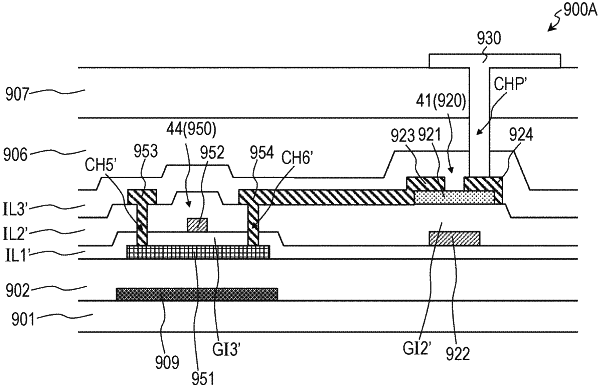
1. An active matrix substrate including a display region and a peripheral region, the display region being defined by pixel regions arranged in a matrix, the peripheral region being located around the display region, the active matrix substrate comprising:
a substrate;
a first insulating layer;
a second insulating layer provided above the first insulating layer;
a first Thin Film Transistor (TFT);
a second TFT disposed in the display region; wherein the first TFT includes:
a silicon semiconductor layer including a first channel region, a first source region, and a first drain region;
a first gate insulating layer being provided above the silicon semiconductor layer;
a first gate electrode being provided above the first gate insulating layer, the first gate electrode opposing the first channel region with the first gate insulating layer therebetween; and
a first electrode being electrically connected to one of the first source region and the first drain region;
the second TFT includes:
an oxide semiconductor layer including a second channel region, a second source region, and a second drain region;
a second gate insulating layer being provided above the oxide semiconductor layer;
a second gate electrode being provided above the second gate insulating layer, the second gate electrode opposing the second channel region with the second gate insulating layer therebetween; and
a second electrode being electrically connected to one of the second source region and the second drain region;
the first insulating layer includes the first gate insulating layer;
the second insulating layer includes a portion that covers the first gate electrode and the second gate electrode;
the first electrode and the second electrode are provided above the second insulating layer;
the first electrode is electrically connected to the one of the first source region and the first drain region via a first contact hole defined in the first insulating layer and the second insulating layer; and
the second electrode is electrically connected to the one of the second source region and the second drain region via a second contact hole defined in the second insulating layer.
|