| CPC G09G 3/3648 (2013.01) [G09G 3/3611 (2013.01); H01L 27/1225 (2013.01); G09G 2300/0408 (2013.01); G09G 2330/022 (2013.01); G09G 2340/0435 (2013.01); G09G 2360/14 (2013.01)] | 10 Claims |
|
1. An electronic device comprising:
a first housing;
a second housing;
a first display portion overlapping with the first housing;
a second display portion overlapping with the second housing; and
a hinge portion connecting the first housing and the second housing,
wherein each of the first display portion and the second display portion comprises:
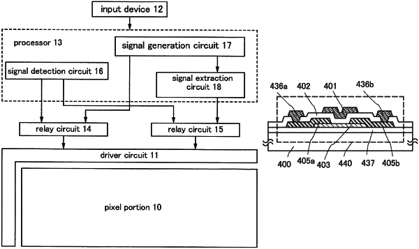
a semiconductor layer over a first insulating layer;
source and drain electrodes over the semiconductor layer, one of the source and drain electrodes being in contact with a first side surface of the semiconductor layer and the other of the source and drain electrodes being in contact with a second side surface of the semiconductor layer;
a second insulating layer over the semiconductor layer and the source and drain electrodes;
a gate electrode overlapping with the semiconductor layer; and
a conductive layer over and in contact with the one of the source and drain electrodes through an opening in the second insulating layer,
wherein the first display portion is larger than the second display portion,
wherein the electronic device is able to be changed in a folded state and an opened state along with the hinge portion, and
wherein the electronic device is capable of wireless communication.
|