| CPC G09G 3/3283 (2013.01) [G09G 3/3233 (2013.01); G09G 2300/0426 (2013.01); G09G 2300/0819 (2013.01); G09G 2300/0842 (2013.01); G09G 2300/0861 (2013.01); G09G 2310/08 (2013.01)] | 16 Claims |
|
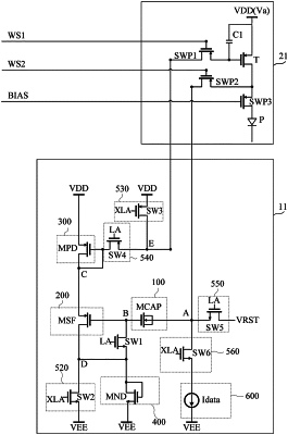
1. A source driving circuit, comprising:
a voltage isolation circuit, a voltage follower circuit, a first voltage dividing circuit, a second voltage dividing circuit, a first switch circuit, a second switch circuit, a third switch circuit, a fourth switch circuit, a fifth switch circuit, a sixth switch circuit and a current source;
wherein the voltage isolation circuit is electrically connected between a first node and a second node and is configured to isolate a voltage of the first node from a voltage of the second node;
wherein a first terminal of the voltage follower circuit is electrically connected to the second node, a second terminal of the voltage follower circuit is electrically connected to a third node, a third terminal of the voltage follower circuit is electrically connected to a fourth node, and the voltage follower circuit is configured to set a voltage of the third node to be varied with the voltage of the second node in a data write stage;
wherein the first voltage dividing circuit is electrically connected between the third node and a positive power supply signal terminal, and the first voltage dividing circuit is configured to adjust the voltage of the third node;
wherein the second voltage dividing circuit is electrically connected between the fourth node and a negative power supply signal terminal, and the second voltage dividing circuit is configured to adjust a voltage of the fourth node;
wherein the first switch circuit is electrically connected between the second node and the fourth node, and the first switch circuit is configured to form a conductive pathway between the second node and the fourth node in a reset and initialization stage;
wherein the second switch circuit is electrically connected between the fourth node and the negative power supply signal terminal, and the second switch circuit is configured to form a conductive pathway between the fourth node and the negative power supply signal terminal in the data write stage;
wherein the third switch circuit is electrically connected between a fifth node and the positive power supply signal terminal, the fifth node and the first node are electrically connected to a drive transistor of a pixel driving circuit, and the third switch circuit is configured to form a conductive pathway between the fifth node and the positive power supply signal terminal in the reset and initialization stage;
wherein the fourth switch circuit is electrically connected between the third node and the fifth node and is configured to form a conductive pathway between the third node and the fifth node in the data write stage;
wherein the fifth switch circuit is electrically connected between the first node and a reset signal terminal and is configured to form a conductive pathway between the first node and the reset signal terminal in the reset and initialization stage; and
wherein the sixth switch circuit is electrically connected between the first node and the current source, and the sixth switch circuit is configured to form a conductive pathway between the first node and the current source in the data write stage;
wherein the current source is electrically connected between the sixth switch circuit and the negative power supply signal terminal and is configured to provide a data current.
|