| CPC G09G 3/3266 (2013.01) [G09G 3/2003 (2013.01); G09G 2310/0262 (2013.01); G09G 2310/0289 (2013.01); G09G 2330/12 (2013.01)] | 18 Claims |
|
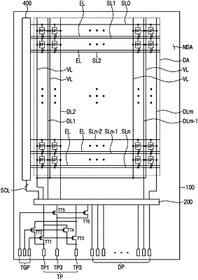
1. A display device, comprising:
a plurality of first pixels connected to a plurality of first scan lines and including a first pixel connected to a first data line and a fourth pixel connected to a third data line;
a plurality of second pixels connected to a plurality of second scan lines and including a second pixel connected to the first data and a fifth pixel connected to the third data line;
a plurality of third pixels connected to the first scan lines or the second scan lines and including a third pixel connected to a second data line;
a scan driver including a first scan driving circuit and a second scan driving circuit disposed opposite to each other;
a first test transistor which supplies a first lighting voltage to the list data line based on a first test gate signal;
a second test transistor which supplies the first lighting voltage to the third data line based on a second test gate signal; and
a third test transistor which supplies a third lighting voltage to the third data line based on the first test gate signal,
wherein each of the first scan driving circuit and the second scan driving circuit comprises:
a plurality of first stages connected to the first scan lines and a first start signal line, wherein the plurality of first stages supplies a plurality of first scan signals to the first scan lines, the plurality of first scan signals including a first on-period having a first voltage to turn on first transistors connected to the first scan lines and a first off-period having a second voltage to turn off the first transistors; and
a plurality of second stages connected to the second scan lines and a second start signal line different from the first start signal line, wherein the plurality of second stages are not connected to the first scan lines and supplies a plurality of second scan signals to the second scan lines, the plurality of second scan signals including a second on-period having a third voltage to turn on second transistors connected to the second scan lines and a second off-period having a fourth voltage to turn off the fourth transistors,
wherein the first on-period of the first scan signals from the first stages and the second on-period of the second scan signals from the second stages do not overlap each other, and
output terminals of the second stages are not connected to output terminals of the first stages.
|