| CPC G09G 3/3233 (2013.01) [H10K 59/131 (2023.02); G09G 2300/0426 (2013.01); G09G 2300/0452 (2013.01); G09G 2300/0819 (2013.01); G09G 2300/0842 (2013.01); G09G 2310/08 (2013.01); G09G 2330/021 (2013.01)] | 20 Claims |

|
1. A display substrate, comprising:
a base substrate, comprising a display region, wherein the display region comprises a plurality of sub-pixels, and each of the plurality of sub-pixels comprises a pixel driving circuit and a light-emitting element, the light-emitting element comprises a light-emitting region and a first electrode located in the light-emitting region of the light-emitting element, the pixel driving circuit is configured to drive the light-emitting element to emit light,
wherein the pixel driving circuit comprises a driving sub-circuit, a data writing sub-circuit, a compensation sub-circuit, and a storage sub-circuit, a first light emission control sub-circuit and a second light emission control sub-circuit, a first reset sub-circuit and a second reset sub-circuit,
the driving sub-circuit is electrically connected to a first node and a second node, and is configured to control a driving current flowing through the light-emitting element under a control of a level of the first node;
the data writing sub-circuit is electrically connected to the second node, and is configured to receive a scanning signal and write a data signal to the driving sub-circuit in response to the scanning signal;
the compensation sub-circuit is electrically connected to the first node and a third node, and is configured to receive the scanning signal and perform threshold compensation on the driving sub-circuit in response to the scanning signal;
the storage sub-circuit is electrically connected to the first node and is configured to store the data signal;
the first light emission control sub-circuit is electrically connected to the second node, and is configured to apply the first power supply voltage to the driving sub-circuit in response to a light emission control signal;
the second light emission control sub-circuit is electrically connected to the third node and a fourth node, and is configured to enable the driving current to be applied to the light-emitting element in response to the light emission control signal;
the first reset sub-circuit is electrically connected to the first node, and is configured to apply a first reset voltage to the first node in response to a first reset control signal;
the second reset sub-circuit is electrically connected to the fourth node, and is configured to apply a second reset voltage to the fourth node in response to a second reset control signal;
the driving sub-circuit comprises a first transistor, the data writing sub-circuit comprises a second transistor, the compensation sub-circuit comprises a third transistor, and the storage sub-circuit comprises a storage capacitor, the first light emission control sub-circuit comprises a fourth transistor, the second light emission control sub-circuit comprises a fifth transistor, the first reset sub-circuit comprises a sixth transistor, the second reset sub-circuit comprises a seventh transistor,
a plurality of reset signal lines, extending along a first direction, and each of the plurality of reset signal lines is electrically connected to the pixel driving circuits of the plurality of sub-pixels located in one row in one-to-one correspondence to provide a reset signal;
a first electrode layer, comprising a plurality of first power supply voltage lines, a plurality of first signal lines, a plurality of first transfer electrodes, a plurality of second transfer electrodes and a plurality of third transfer electrodes,
each of the first transfer electrodes, each of the second transfer electrodes, and each of the third transfer electrodes are located in the pixel driving circuit of each of the plurality of sub-pixels,
wherein the plurality of first power supply voltage lines extend along a second direction different from the first direction, the plurality of first power supply voltage lines are electrically connected to the pixel driving circuits of the plurality of sub-pixels, and the plurality of first power supply voltage lines are configured to provide the first power supply voltages to the pixel driving circuits,
the plurality of first signal lines extend along the second direction and are arranged side by side with the plurality of first power supply voltage lines, and the plurality of first signal lines are configured to provide first display signals to the pixel driving circuits of the plurality of sub-pixels,
each of the first transfer electrodes extends along the second direction and is electrically connected to the first transistor and the third transistor,
each of the second transfer electrodes extends along the second direction and is electrically connected to the sixth transistor and the reset signal line,
each of the third transfer electrodes is electrically connected to the fifth transistor and the light-emitting element,
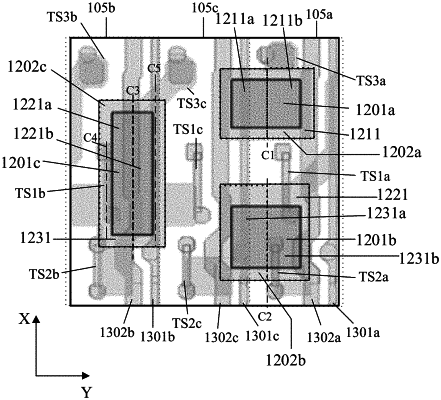
wherein the first electrode of each of the plurality of sub-pixels comprises a body portion, the body portion comprises a first body sub-portion and a second body sub-portion, and the first body sub-portion and the second body sub-portion are located at two sides of a center line extending in the second direction of the body portion,
a value of a ratio of an area of an overlapping portion of an orthographic projection of the first body sub-portion on a board surface of the base substrate and an orthographic projection of the first electrode layer on the board surface of the base substrate, to an area of an overlapping portion of an orthographic projection of the second body sub-portion on the board surface of the base substrate and the orthographic projection of the first electrode layer on the board surface of the base substrate ranges from 0.82 to 1.02.
|