| CPC G09G 3/32 (2013.01) [G09G 3/3233 (2013.01); G09G 2300/0852 (2013.01); G09G 2310/0267 (2013.01); G09G 2310/0275 (2013.01); G09G 2320/0233 (2013.01); G09G 2330/021 (2013.01)] | 20 Claims |
|
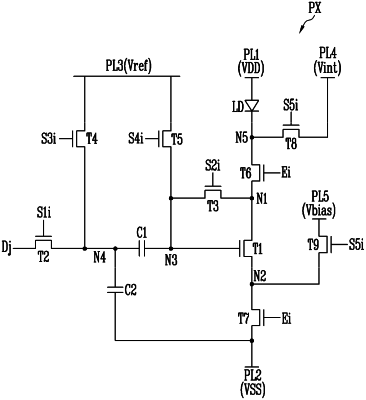
1. A pixel comprising:
a light emitting element including a first electrode and a second electrode;
a first transistor connected between a first node and a second node, and configured to generate driving current flowing from a first power line for providing a first power voltage to a second power line for providing a second power voltage via the light emitting element;
a second transistor connected between a data line and a fourth node, and configured to be turned on in response to a first scan signal supplied to a first scan line;
a third transistor connected between the first node and a third node corresponding to a gate electrode of the first transistor, and configured to be turned on in response to a second scan signal supplied to a second scan line;
a fourth transistor connected between the fourth node and a third power line for providing a third power voltage, and configured to be turned on in response to a third scan signal supplied to a third scan line;
a fifth transistor connected between the third node and the third power line, and configured to be turned on in response to a fourth scan signal supplied to a fourth scan line;
a sixth transistor connected between the first node and a fifth node corresponding to the second electrode of the light emitting element, and configured to be turned off in response to an emission control signal supplied to an emission control line;
a seventh transistor connected between the second node and the second power line, and configured to be turned off in response to the emission control signal; and
a first capacitor connected between the third node and the fourth node.
|