| CPC G09G 3/32 (2013.01) [G09G 2300/026 (2013.01); G09G 2310/0262 (2013.01); G09G 2310/0267 (2013.01); G09G 2310/08 (2013.01); G09G 2320/0646 (2013.01)] | 15 Claims |
|
1. A display device, comprising:
a plurality of pixel units arranged in a matrix of rows and columns, each of the plurality of pixel units including a light emitter and a pixel circuit, the light emitter being configured to emit light with a luminance level changeable in response to a level of a current, the pixel circuit being configured to cause the light emitter to emit light with a luminance level corresponding to a tone resulting from an image signal,
wherein the pixel circuit includes
a low-tone driver configured to drive the light emitter in response to a tone resulting from an image signal being within a low-tone range of tones below or equal to a predetermined tone, and not to drive the light emitter in response to a tone resulting from an image signal being within a high-tone range of tones above the predetermined tone, and
a high-tone driver configured not to drive the light emitter in response to a tone resulting from an image signal being within the low-tone range, and to drive the light emitter in response to a tone resulting from an image signal being within the high-tone range;
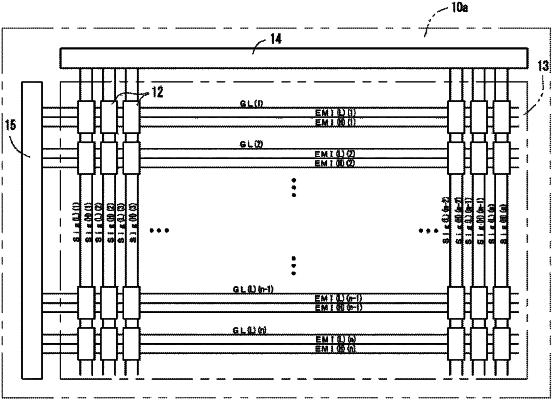
a data signal line for each column of the matrix of the plurality of pixel units;
a first power supply line configured to receive a power supply voltage;
a second power supply line configured to receive a power supply voltage lower than the power supply voltage for the first power supply line;
a low-tone scanning line for each row of the matrix;
a low-tone emission control line for each row of the matrix;
a high-tone scanning line for each row of the matrix;
a high-tone emission control line for each row of the matrix;
a signal line drive circuit configured to output an image signal to the data signal line; and
a scanning line drive circuit configured to output a selection signal to the low-tone scanning line and to the high-tone scanning line,
wherein the low-tone driver includes
a low-tone scanning transistor including a gate terminal connected to the low-tone scanning line and a source terminal connected to the data signal line,
a low-tone capacitor including a first terminal connected to a drain terminal of the low-tone scanning transistor and a second terminal connected to the first power supply line,
a low-tone drive transistor including a gate terminal connected to the first terminal of the low-tone capacitor and a source terminal connected to the first power supply line, and
a low-tone emission control transistor including a gate terminal connected to the low-tone emission control line, a drain terminal connected to an anode of the light emitter, and a source terminal connected to a drain terminal of the low-tone drive transistor,
the high-tone driver includes
a high-tone scanning transistor including a gate terminal connected to the high-tone scanning line and a source terminal connected to the data signal line,
a high-tone capacitor including a first terminal connected to a drain terminal of the high-tone scanning transistor and a second terminal connected to the first power supply line,
a high-tone drive transistor including a gate terminal connected to the first terminal of the high-tone capacitor and a source terminal connected to the first power supply line, and
a high-tone emission control transistor including a gate terminal connected to the high-tone emission control line, a drain terminal connected to the anode of the light emitter, and a source terminal connected to a drain terminal of the high-tone drive transistor, and
the light emitter is connected between the drain terminal of the low-tone emission control transistor and the second power supply line and between the drain terminal of the high-tone emission control transistor and the second power supply line.
|