| CPC G09G 3/32 (2013.01) [G09G 3/3426 (2013.01); G09G 2300/0814 (2013.01); G09G 2300/0842 (2013.01); G09G 2310/08 (2013.01); G09G 2320/0233 (2013.01); G09G 2320/0257 (2013.01); G09G 2320/064 (2013.01); G09G 2320/066 (2013.01); G09G 2320/0633 (2013.01)] | 18 Claims |
|
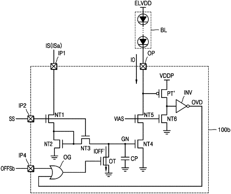
1. A display device comprising:
a light-emitting diode (LED) backlight unit (BLU);
a pixel driving circuit configured to generate a scan signal and an image signal; and
a pixel circuit configured to generate an output current based on the scan signal and the image signal, and transmit the output current to the LED BLU,
the pixel circuit including,
a transistor configured to generate the output current according to a voltage of a gate node,
a capacitor connected to the gate node, and
a second transistor configured to discharge the gate node in response to detection of a voltage of an output current pin exceeding a reference voltage.
|