| CPC G09G 3/32 (2013.01) [G09G 2310/0278 (2013.01)] | 12 Claims |
|
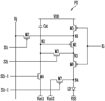
1. A pixel comprising:
a light emitting device;
a first transistor including a first electrode connected to a first node electrically connected to a first power source, and controlling a driving current based on a voltage of a second node;
a second transistor connected between a data line and the first node, and turned on in response to a first scan signal;
a third transistor connected between a third node connected to a second electrode of the first transistor and the second node, and turned on in response to a second scan signal;
a fourth transistor connected between the third node and an initialization power source, and turned on in response to the second scan signal;
a fifth transistor connected between the first power source and the first node, and turned off in response to an emission control signal; and
a sixth transistor connected between the third node and a first electrode of the light emitting device, and turned off with the fifth transistor,
wherein the second transistor is electrically connected to a first scan line, the first scan signal being supplied to the first scan line at a first frequency,
wherein the fourth transistor is electrically connected to a second scan line, the second scan signal being supplied to the second scan line at a second frequency, the second frequency being different from the first frequency,
wherein an inspection signal is supplied to the data line in response to the first scan signal in a first period, and
wherein a bias signal is supplied to the first transistor through the data line in response to the first scan signal in a second period.
|