| CPC G06F 30/392 (2020.01) [G06F 30/394 (2020.01); G06F 30/398 (2020.01)] | 13 Claims |
|
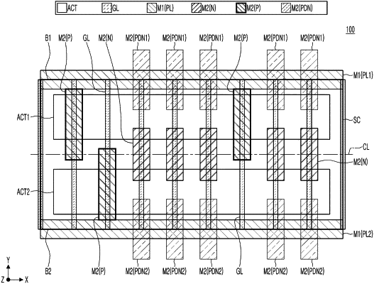
1. A semiconductor device comprising:
a standard cell comprising:
an active region extending in a first direction on a substrate;
a gate structure intersecting the active region and extending in a second direction intersecting the first direction;
a first conductive structure comprising:
a first power supply line and a second power supply line disposed on the active region and the gate structure and extending in the first direction; and
signal lines disposed between the first power supply line and the second power supply line; and
a second conductive structure disposed on the first conductive structure, the second conductive structure comprising:
first power distribution patterns spaced apart from each other in the first direction along a first boundary of the standard cell and electrically connected to the first power supply line;
second power distribution patterns spaced apart from each other in the first direction along a second boundary of the standard cell and electrically connected to the second power supply line;
net metal lines disposed between and spaced apart from the first power distribution patterns and the second power distribution patterns, and electrically connected to a first portion of the signal lines; and
pin metal lines electrically connected to a second portion of the signal lines, and extending in the second direction,
wherein the first boundary corresponds to the first power supply line and the second boundary corresponds to the second power supply line,
wherein each of the net metal lines has a center disposed on a central axis extending in the first direction between the first boundary and the second boundary,
wherein, along the second direction, a first distance between the central axis and the first power supply line is substantially equal to a second distance between the central axis and the second power supply line, and
wherein at least one of the pin metal lines is disposed closer to the first boundary or the second boundary than the net metal lines.
|