| CPC G06F 30/3312 (2020.01) [G06F 30/3315 (2020.01); G06F 2119/12 (2020.01)] | 6 Claims |
|
1. A flexible modeling method for a timing constraint of a register, including the following steps:
step 1. performing simulation in a case of each combination of SQ, Tdi, Tckj, and CLk respectively to obtain a timing constraint range for establishing a model, where SQ represents an output terminal state of a register; Tdi represents p types of input terminal transition time Td of the register, i is an integer, and 1≤i≤p; Tckj represents q types of clock terminal transition time Tck of the register, j is an integer, and 1≤j≤q; and CLk represents m types of output load capacitance CL of the register, k is an integer, and 1≤k≤m;
step 2. under the obtained timing constraint range under each combination of SQ, Tdi, Tckj, and CLK, setting that Tstep is a sampling interval of both setup slack and hold slack, extracting N combination pairs of setup slack Tsu and hold slack Thd with the set Tstep as intervals for both setup slack and hold slack, performing simulation by using a transistor-level simulation tool to respectively obtain N clock terminal-to-output terminal delays of the register, and subsequently combining all simulation data of under all combinations of SQ, Tdi, Tckj, and CLK together to obtain Ns groups of model training sample data, where each group of training sample data includes parameters including the input terminal transition time, the clock terminal transition time, the output load capacitance, the setup slack, the hold slack, the output terminal state, and the clock terminal-to-output terminal delay of the register, where N is an integer which denotes the number of combinations for simulation with different Tsu and Thd under the same set of SQ, Tdi, Tckj, and CLK, Ns is an integer which denotes the number of samples for model training with different SQ, Tdi, Tckj, and CLk as well as Tsu and Thd and Tsu and Thd denote the time of setup slack and hold slack respectively;
step 3. using the input terminal transition time, the clock terminal transition time, the output load capacitance, the setup slack, the hold slack, and the output terminal state of the register as model features, using the corresponding clock terminal-to-output terminal delays of the register obtained in step 2 as model labels, performing training by using a neural network, and establishing a mutually independent timing model of the register; and
step 4. obtaining timing constraints by using a static timing analysis tool, the timing constraints including the output terminal state, the input terminal transition time, the clock terminal transition time, and the output load capacitance of the register, and performing inference by using the mutually independent timing model of the register obtained in step 3 to obtain a clock terminal-to-output terminal delay of the register when the setup slack is Tsut and a clock terminal-to-output terminal delay of the register when the hold slack is Thdt,
wherein step 1 includes the following steps:
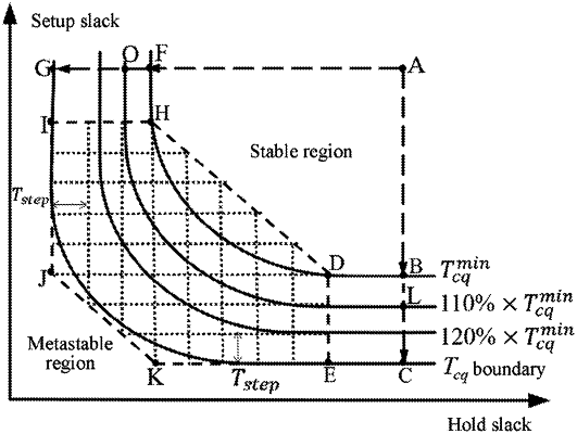
step 1.1. under each combination of SQ, Tdi, Tckj, and CLK, performing simulation by using the transistor-level simulation tool first to obtain clock terminal-to-output terminal delays Tcq when the setup slack has a sufficiently large value Tsu(max) and the hold slack has a sufficiently large value Thd(max), where the sufficiently large value of the setup slack refers to that in this case, if Tsu continues to increase, Tcq no longer continues to decrease, and the sufficiently large value of the hold slack refers to that in this case, if Thd continues to increase, Tcq no longer continues to decrease, that is, when the setup slack increases from Tsu(max) to δsu×Tsu(max) and the hold slack increases from Thd(max) to δhd×Thd(max), Tcq remains unchanged, where δsu is a setup slack verification coefficient, 1≤δsu≤1.1, δhd is a hold slack verification coefficient, 1≤δhd≤1.1, and in this case, the register operates in a stable region, and it is denoted in this case that Tcq is Tcqmin in the hold slack is ThdA, and the setup slack is TsuA;
step 1.2. gradually reducing the setup slack with ThdA as a fixed hold slack, where setup slack obtained when transistor-level simulation fails is minimum setup slack in the timing constraint range, and it is denoted in this case that the setup slack is TsuC;
step 1.3. searching for the value of the setup slack by using a binary method with ThdA as a fixed hold slack, where an interval in which the search is started is [TsuC, TsuA], performing simulation on the setup slack by using the transistor-level simulation tool to obtain Tcq, and setting a target value of Tcq to Bcq×Tcqmin, where Bcq is a first target coefficient of the setup slack, 1≤Bcq≤1.1, and the value of the setup slack found through binary search is denoted as TsuB;
step 1.4. gradually reducing the hold slack with TsuA as a fixed setup slack, where hold slack obtained when transistor-level simulation fails is minimum hold slack in the timing constraint range, and it is recorded in this case that the hold slack is ThdG;
step 1.5. searching for the value of the hold slack by using a binary method with TsuA as a fixed setup slack, where an interval in which the search is started is [ThdG, ThdA], performing simulation on the hold slack by using the transistor-level simulation tool to obtain the clock terminal-to-output terminal delay Tcq, and setting a target value of the clock terminal-to-output terminal delay Tcq to Fcq×Tcqmin where Fcq is a first target coefficient of the hold slack, 1≤Fcq≤1.1, and the value of the hold slack found through binary search is denoted as ThdF; and
step 1.6. searching for the value of the hold slack by using a binary method with TsuB as a fixed setup slack, where an interval in which the search is started is [ThdF, ThdA], performing simulation on the hold slack by using the transistor-level simulation tool to obtain the clock terminal-to-output terminal delay Tcq, and setting the target value of the clock terminal-to-output terminal delay Tcq to Dcq×Tcqmin, where Dcq is a second target coefficient of the hold slack, Bcq≤Dcq≤1.1, and the value of the hold slack found through binary search is denoted as ThdD;
step 1.7. searching for the value of the setup slack by using a binary method with ThdF as a fixed hold slack, where an interval in which the search is started is [TsuB, TsuA], performing simulation on the setup slack by using the transistor-level simulation tool to obtain the clock terminal-to-output terminal delay Tcq, and setting the target value of the clock terminal-to-output terminal delay Tcq to Hcq×Tcqmin, where Hcq is a second target coefficient of the setup slack, Fcq≤Hcq≤1.1, and the value of the setup slack found through binary search is denoted as TsuH;
step 1.8. forming a constraint condition by using the following formulas for a simulation range of the pair of the hold slack Thd and the setup slack Tsu under the combination of SQ, Tdi, Tckj, and CLK;
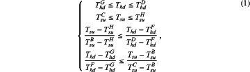 the foregoing formula is the timing constraint range of the model established in a case of the combination of SQ, Tdi, Tckj, and CLk.
|