| CPC G06F 13/4027 (2013.01) [G06F 13/4282 (2013.01)] | 20 Claims |
|
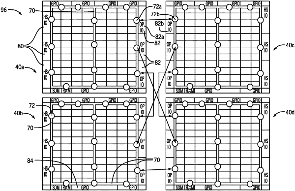
1. An integrated circuit device, comprising:
a first network on chip (NOC) circuit configurable to:
receive a set of data; and
transfer the set of data to a first node of the first NOC circuit, wherein the first node is configured to directly transfer the set of data to a second node of a second NOC circuit of an additional integrated circuit device separate from the integrated circuit device, and wherein the first node comprises a first protocol translator configurable to translate a first protocol associated with the first NOC circuit into a second protocol associated with an interconnection resource of a plurality of interconnection resources configurable for off-die communication; and
the second NOC circuit configurable to:
receive the set of data from the second node, wherein the second node is associated with the interconnection resource of the plurality of interconnection resources, and wherein the second node comprises a second protocol translator configurable to translate the second protocol associated with the interconnection resource into a third protocol associated with the second NOC circuit.
|