US 11,789,879 B2
Memory device supporting a high-efficient input/output interface and a memory system including the memory device
Hyungmin Jin, Seoul (KR); Jindo Byun, Suwon-si (KR); Younghoon Son, Yongin-si (KR); Youngdon Choi, Seoul (KR); and Junghwan Choi, Hwaseong-si (KR)
Assigned to SAMSUNG ELECTRONICS CO., LTD., Suwon-si (KR)
Filed by SAMSUNG ELECTRONICS CO., LTD., Suwon-si (KR)
Filed on Sep. 6, 2022, as Appl. No. 17/903,240.
Application 17/903,240 is a continuation of application No. 17/326,513, filed on May 21, 2021, granted, now 11,461,251.
Claims priority of application No. 10-2020-0134639 (KR), filed on Oct. 16, 2020.
Prior Publication US 2022/0414032 A1, Dec. 29, 2022
This patent is subject to a terminal disclaimer.
Int. Cl. G06F 13/16 (2006.01); H04L 25/49 (2006.01)
CPC G06F 13/1668 (2013.01) [H04L 25/4917 (2013.01)] 20 Claims
OG exemplary drawing
 
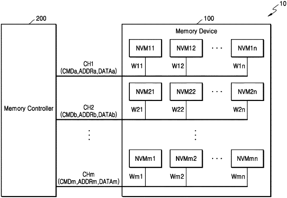
1. A memory system, comprising:
a memory controller configured to:
transmit a command or an address to a first channel based on a data input/output signal having one of N (N is a natural number of three or more) different voltage levels, and
transmit data to the first channel based on the data input/output signal having one of two different voltage levels; and
a memory device configured to:
sample the command or the address received via the first channel in a pulse amplitude modulation (PAM)-N mode, and
sample the data received via the first channel in a non return to zero (NRZ) mode.