| CPC G06F 11/1068 (2013.01) [G06F 3/0619 (2013.01); G06F 3/0656 (2013.01); G06F 3/0679 (2013.01); G06F 11/0772 (2013.01); H03K 19/21 (2013.01)] | 20 Claims |
|
1. A memory device comprising:
a memory module including a memory array, wherein the memory array includes a plurality of memory cells; and
a memory controller that retrieves read data from memory cells among the plurality of memory cells,
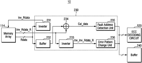
wherein the memory controller includes a fault detector that detects faulty addresses associated with faulty memory cells among the memory cells providing data errors, and
the fault detector comprises:
a first inverter that generates inverted read data by reading and inverting the read data, wherein the inverted read data is stored in the memory array;
a first buffer that stores the read data and provides buffered data;
an XOR operator that receives the buffered data from the first buffer, receives read-out inverted data generated by reading the inverted read data stored in the memory array, and performs an XOR operation on the buffered data and the read-out inverted read data to generate calculation data;
a fault address detection unit that identifies the faulty addresses in response to the calculation data and generates faulty address information;
a second inverter that generates inverted read-out inverted read data by receiving and inverting the read-out inverted read data; and
an error pattern change unit that converts an uncorrectable error (UE)-causing data into a correctable error (CE)-causing data.
|