| CPC G06F 3/0605 (2013.01) [G06F 3/0611 (2013.01); G06F 3/0625 (2013.01); G06F 3/0635 (2013.01); G06F 3/0659 (2013.01); G06F 3/0673 (2013.01); G06F 9/30196 (2013.01); G06F 15/785 (2013.01); Y02D 10/00 (2018.01)] | 20 Claims |
|
1. A memory device comprising:
a first memory portion for translating a memory command into a logic command to perform an arithmetic operation; and
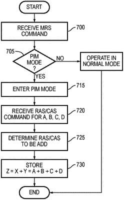
an interface for receiving a configuration command from a host to configure the memory device to operate in a processor-in-memory (PIM) mode,
wherein the memory device, operating in the PIM mode and receiving at least one of a “read” command, an “activate” command, a “precharge” command, or a “refresh” command as the memory command, is configured to compute data by performing a memory access operation comprising at least one of an “add” command, a “multiply” command, a “divide” command, a “compare” command, a “shift” command, an “and” command, an “or” command, or an “xor” command as the logic command.
|