| CPC G06F 3/0445 (2019.05) [G06F 3/04164 (2019.05)] | 20 Claims |
|
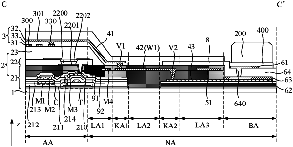
1. A display panel having a display region and a non-display region, the non-display region comprising a line arranging region and a binding region, the display panel comprising:
touch electrodes located in the display region and in a touch layer;
pixel units located in the display region and in a display layer;
power supply voltage signal lines located in the display region;
touch lines located in the line arranging region;
power supply voltage lines located in the line arranging region and electrically connected to the power supply voltage signal lines; and
touch bonding pads located in the binding region and electrically connected to the touch electrodes through the touch lines,
wherein the touch layer is located on a side of the display layer facing away from a substrate, the line arranging region comprises a first line arranging region, a second line arranging region and a third line arranging region, the second line arranging region is located between the first line arranging region and the third line arranging region, and the first line arranging region is located at a side of the second line arranging region close to the display region;
wherein the touch lines comprise a first touch line located in the first line arranging region, at least one second touch line located in the second line arranging region, and at least one third touch line located in the third line arranging region, wherein the first touch line is located in the touch layer, and the at least one second touch line and the at least one third touch line are located in the display layer; and
wherein the power supply voltage lines comprise at least one first power supply voltage line, wherein the at least one third touch line is disposed in a layer different from a layer where the at least one first power supply voltage line is disposed, and one of the at least one third touch line at least partially overlaps with one of the at least one first power supply voltage line along a direction perpendicular to a plane of the display panel, and an orthographic projection of the one of the at least one first power supply voltage line onto the plane of the display panel totally covers an orthographic projection of the one of the at least one third touch line onto the plane of the display panel.
|