| CPC G06F 3/044 (2013.01) [G02B 6/4298 (2013.01); G06F 3/042 (2013.01); G06F 2203/04102 (2013.01); G06V 40/1318 (2022.01)] | 14 Claims |
|
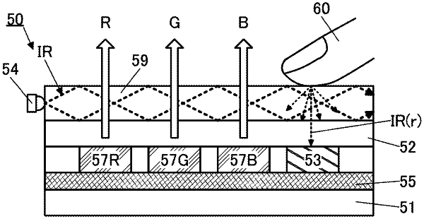
1. A display device comprising:
a first substrate;
a light guide plate;
a first light-emitting element;
a second light-emitting element; and
a light-receiving element,
wherein the first substrate and the light guide plate are provided to face each other,
wherein the first light-emitting element and the light-receiving element which are provided on the same plane are provided between the first substrate and the light guide plate,
wherein the first light-emitting element is configured to emit first light through the light guide plate,
wherein the second light-emitting element is configured to emit second light to a side surface of the light guide plate,
wherein the light-receiving element is configured to receive the second light and to convert the second light into an electric signal,
wherein the first light includes visible light, and
wherein the second light includes infrared light.
|