| CPC G02F 1/136227 (2013.01) [G02F 1/1368 (2013.01); G02F 1/13439 (2013.01); G02F 1/133345 (2013.01); G02F 1/133512 (2013.01); G02F 1/133514 (2013.01); G02F 1/134363 (2013.01); G02F 1/136213 (2013.01); G02F 1/136286 (2013.01); G02F 1/13629 (2021.01)] | 15 Claims |
|
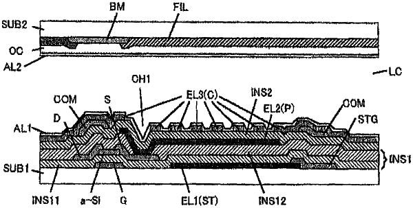
1. A display device comprising:
a first substrate;
an organic insulating film on the first substrate;
a first inorganic insulating film laminated on the organic insulating film;
a signal line between the first substrate and the organic insulating film;
a thin film transistor between the first substrate and the organic insulating film;
a second inorganic insulating film laminated on the first inorganic insulating film;
an alignment film covering the second inorganic insulating film;
a first transparent pixel electrode between the organic insulating film and the alignment film;
a first transparent counter electrode between the organic insulating film and the alignment film;
a metal wiring between the organic insulating film and the alignment film; and a thin film transistor between the first substrate and the organic insulating film, wherein
the metal wiring is connected to the first transparent counter electrode, the organic insulating film is between the first substrate and the first inorganic insulating film,
the first inorganic insulating film is between the organic insulating film and the second inorganic insulating film,
the second inorganic insulating film is between the first inorganic insulating film and the alignment film,
the first transparent pixel electrode is connected to a source electrode of the thin film transistor at a region where the organic insulating film is not formed, a drain electrode of the thin film transistor is a part of the signal line,
the drain electrode is between the first substrate and the organic insulating film,
the first transparent pixel electrode is connected to the source electrode of the thin film transistor at a region where the organic first inorganic insulating film is not formed,
the metal wiring is between the organic insulating film and the first inorganic insulating film, and
a part of the metal wiring overlaps the drain electrode of the thin film transistor.
|