| CPC G02F 1/136204 (2013.01) [G02F 1/1339 (2013.01); G02F 1/134309 (2013.01); G02F 1/133514 (2013.01); G02F 1/136222 (2021.01); G02F 2202/16 (2013.01)] | 20 Claims |
|
1. A liquid crystal display apparatus, comprising:
an active matrix substrate;
a counter substrate opposing the active matrix substrate;
a liquid crystal layer provided between the active matrix substrate and the counter substrate; and
a sealing portion provided between the active matrix substrate and the counter substrate and surrounding the liquid crystal layer,
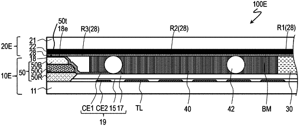
wherein the active matrix substrate includes a first substrate and a first transparent conductive layer supported by the first substrate,
the counter substrate includes a second substrate and a second transparent conductive layer supported by the second substrate,
the active matrix substrate further includes a capacitance element disposed at an outer side of the sealing portion or disposed at least partially overlapping with the sealing portion in a view from a normal direction of the first substrate, the capacitance element including a first capacitance electrode included in the first transparent conductive layer, a second capacitance electrode disposed opposing the first capacitance electrode between the first capacitance electrode and the first substrate, and a dielectric layer located between the first capacitance electrode and the second capacitance electrode,
one of the active matrix substrate and the counter substrate further includes a projection structure disposed at an outer side of the sealing portion, provided between the first substrate and the first transparent conductive layer or between the second substrate and the second transparent conductive layer, and projecting toward a side of the other one of the active matrix substrate and the counter substrate,
the second transparent conductive layer includes a first section present in a region surrounded by the sealing portion, a second section overlapping with the sealing portion in a view from a normal direction of the second substrate, and a third section present at an outer side of the sealing portion, and
the third section of the second transparent conductive layer is in contact with the first transparent conductive layer on a top face of the projection structure.
|