| CPC G02F 1/133555 (2013.01) [B82Y 20/00 (2013.01); G02F 1/1333 (2013.01); G02F 1/1368 (2013.01); G02F 1/133345 (2013.01); G02F 1/133371 (2013.01); G02F 1/136286 (2013.01); G02F 1/136231 (2021.01); G02F 2202/36 (2013.01)] | 6 Claims |

|
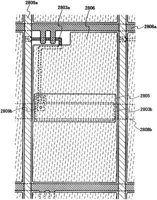
1. A semiconductor device comprising:
a semiconductor film;
a gate insulating film over the semiconductor film;
a gate wiring over and in contact with an upper surface of the gate insulating film;
a first metal film over and in contact with the upper surface of the gate insulating film;
a first insulating film over the gate wiring and the first metal film;
a source line over the first insulating film; and
a second metal film over the first insulating film,
wherein the semiconductor film comprises polycrystalline silicon,
wherein the source line is in direct contact with the semiconductor film,
wherein the semiconductor film comprises a first channel formation region, a second channel formation region, a first region, and a second region;
wherein the gate wiring comprises a third region and a fourth region,
wherein the third region of the gate wiring overlaps the first channel formation,
wherein the fourth region of the gate wiring overlaps the second channel formation,
wherein the first region of the semiconductor film has a first width which is parallel to a direction in which the source line extends, and a second width which is perpendicular to the first width,
wherein the first width of the first region of the semiconductor film is longer than the second width of the first region of the semiconductor film,
wherein the second region of the semiconductor film has a third width which is parallel to a direction in which the source line extends, and a fourth width which is perpendicular to the third width,
wherein the fourth width of the second region of the semiconductor film is longer than the third width of the second region of the semiconductor film,
wherein the first metal film has a fifth width which is parallel to a direction in which the source line extends, and a sixth width which is perpendicular to the fifth width of the first metal film,
wherein the sixth width of the first metal film is longer than the fifth width of the first metal film,
wherein the second metal film overlaps the first metal film with the first insulating film interposed therebetween,
wherein the second metal film overlaps the first region of the semiconductor film,
wherein a long axis of the second metal film is parallel to a long axis of the gate wiring, and
wherein the first insulating film comprises a region which is not overlapped by the second metal film and overlaps the gate insulating film.
|