| CPC G02B 26/085 (2013.01) [B81B 3/0051 (2013.01); B81C 3/00 (2013.01); G02B 7/198 (2013.01); G02B 26/101 (2013.01); B81B 2201/04 (2013.01)] | 26 Claims |
|
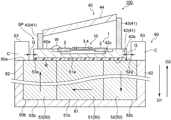
1. An optical module comprising:
a mirror unit having a movable mirror portion including a coil;
a magnet portion having an upper surface, a bottom surface, and a side surface extending from the upper surface to the bottom surface, and configured to generate a magnetic field acting on the movable mirror portion; and
a package accommodating the magnet portion,
wherein the magnet portion is constituted of a plurality of magnets, wherein the package has a bottom wall portion configured to support contact the bottom surface, a side wall portion configured to support contact the side surface, and an upper wall portion configured to support contact the upper surface,
wherein the bottom wall portion and the upper wall portion are connected to each other with the side wall portion, and
wherein the movable mirror portion is disposed in a space formed by the upper surface and the upper wall portion.
|