| CPC G02B 6/0085 (2013.01) [G02F 1/133314 (2021.01); G02F 1/133382 (2013.01); G02F 1/133628 (2021.01); H05K 7/2039 (2013.01); G02B 6/0088 (2013.01)] | 16 Claims |

|
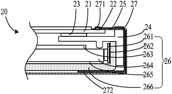
1. A chip heat dissipation structure, wherein the chip heat dissipation structure comprises a chip contact end and a backplate contact end, the chip heat dissipation structure is made of thermal conductive material, the backplate is a backplate of a bottom of a backlight module under a display panel of a liquid crystal display device;
wherein the chip heat dissipation structure comprises:
a first surface serving as a chip contact end, located above the backlight module and the display panel, covering the chip, and contacting the chip in area;
a second surface serving as a backplate contact end, located under the backlight module and the display panel, paralleling the first surface, and contacting the backplate in area; and
a third surface connected a side edge of the first surface opposite to the third surface;
wherein a gap is defined in the second surface and divides the second surface into two portions.
|