| CPC G01T 1/248 (2013.01) [G01T 1/247 (2013.01); H01L 27/0761 (2013.01); H01L 31/103 (2013.01)] | 16 Claims |
|
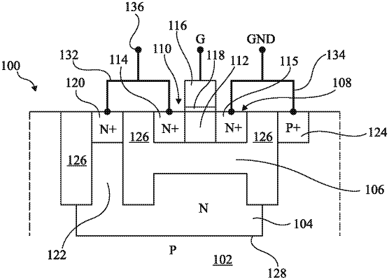
1. A method for detecting an ionizing radiation, comprising:
connecting a first doped region and a second doped region of a PN junction directly to source and drain nodes, respectively, of a first transistor;
in response to said ionizing radiation crossing through both said PN junction and said first transistor:
generating a first current through the PN junction causing a reduction in potential at the first doped region; and
generating a second current through a source-drain path of the first transistor causing a further reduction in potential at the first doped region; and
applying the further reduced potential at the first doped region to a back gate of said first transistor.
|