| CPC G01R 31/318555 (2013.01) [G01R 31/318572 (2013.01)] | 12 Claims |
|
1. An electronic device, comprising:
a processing unit including at least one memory;
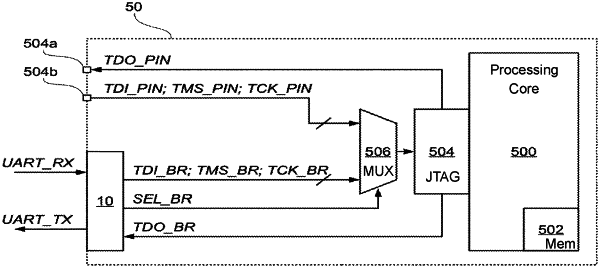
a test interface coupled to said processing unit, the test interface comprising a test data input line and a test mode select line, wherein said at least one memory is accessible via said test interface;
a bridge circuit; and
a multiplexer circuit;
wherein said bridge circuit comprises:
a serial communication interface configured to receive a serial data input signal conveying at least one input serial data frame including a set of input binary values, said set of input binary values comprising a first subset of input binary values and a second subset of input binary values, said first subset of input binary values comprising a first half of the input binary values in said set of input binary values, and said second subset of input binary values comprising a second half of the input binary values in said set of input binary values; and
a serial-to-parallel converter circuit configured to:
receive said at least one input serial data frame from said serial communication interface;
process said at least one input serial data frame to read the first subset of input binary values and the second subset of input binary values from said set of input binary values; and
transmit said first subset of input binary values via a first output signal and transmit said second subset of input binary values via a second output signal; and
wherein the multiplexer circuit is configured to selectively propagate either a test data input signal received at a first pin of the electronic device or said first output signal transmitted by said bridge circuit to the test data input line of the test interface, and to selectively propagate either a test mode select signal received at a second pin of the electronic device or said second output signal transmitted by said bridge circuit to the test mode select line of the test interface.
|