US 11,789,070 B2
Integrated communication link testing
Pirooz Hojabri, San Jose, CA (US); Joshua J. O'Brien, Aloha, OR (US); Gregory A. Martin, Lake Oswego, OR (US); Patrick Satarzadeh, San Jose, CA (US); and Karen Hovakimyan, San Jose, CA (US)
Assigned to Tektronix, Inc., Beaverton, OR (US)
Filed by Tektronix, Inc., Beaverton, OR (US)
Filed on May 18, 2021, as Appl. No. 17/324,007.
Application 17/324,007 is a continuation of application No. 16/440,944, filed on Jun. 13, 2019, granted, now 11,009,546.
Claims priority of provisional application 62/684,784, filed on Jun. 14, 2018.
Prior Publication US 2021/0270893 A1, Sep. 2, 2021
This patent is subject to a terminal disclaimer.
Int. Cl. G06F 11/00 (2006.01); G01R 31/317 (2006.01); G01R 31/28 (2006.01); G01R 31/3187 (2006.01); G01R 31/319 (2006.01)
CPC G01R 31/3171 (2013.01) [G01R 31/2841 (2013.01); G01R 31/3187 (2013.01); G01R 31/31905 (2013.01)] 19 Claims
OG exemplary drawing
 
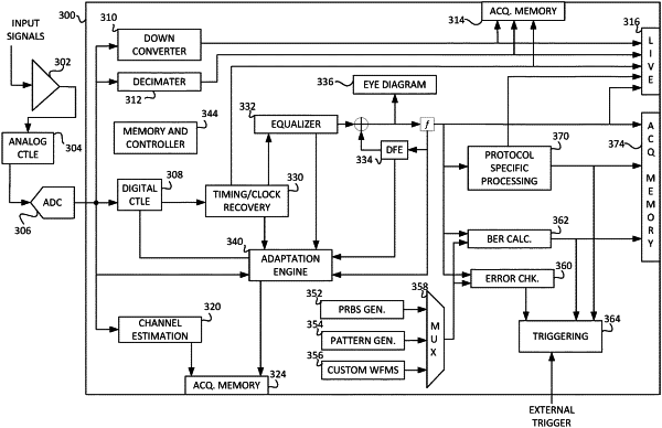
1. A test and measurement device, comprising:
an input configured to receive an analog signal from a Device Under Test (DUT);
an Analog to Digital Converter (ADC) coupled to the input and structured to convert the analog signal to a digital signal;
a receiver structured to accept the digital signal and perform signal conditioning, symbol recovery, and analysis on the digital signal at a rate that is the same or exceeds a baud rate of the analog signal.