| CPC G01R 31/2621 (2013.01) [G01R 31/2851 (2013.01)] | 14 Claims |
|
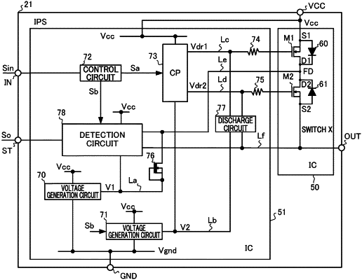
1. An integrated circuit for a semiconductor device that includes
a first terminal for receiving a power supply voltage,
a second terminal to which a load is to be coupled, and
a first metal-oxide-semiconductor (MOS) transistor and a second MOS transistor, each having a drain electrode and a source electrode, the source electrodes of the first and second MOS transistors being respectively coupled to the first and second terminals,
the integrated circuit comprising:
a first line coupled to the drain electrode of the first MOS transistor and the drain electrode of the second MOS transistor;
a second line to which a first voltage lower than the power supply voltage is applied;
a third line coupled to the second terminal;
a first device configured to couple the first line and the second line, to prevent the first line from being brought into a floating state; and
a detection circuit configured to detect a first abnormality in at least the first MOS transistor based on a voltage level of the first line, and to detect a second abnormality in at least the second MOS transistor based on a voltage level of the third line.
|