| CPC G01R 19/1659 (2013.01) [H01H 47/02 (2013.01); H01H 47/325 (2013.01)] | 22 Claims |
|
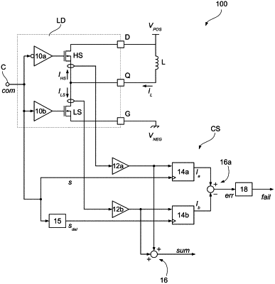
1. A circuit, comprising:
a high-side switch and a low-side switch having an intermediate node intermediate the high-side switch and the low-side switch, wherein the high-side switch is configured to provide a first current flow line between a supply voltage node and the intermediate node and the low-side switch is configured to provide a second current flow line between the intermediate node and a reference voltage node;
a control input node configured to receive a switching control signal, the switching control signal being applied with opposite polarities to the high-side switch and the low-side switch, wherein the high-side switch and the low-side switch are configured to drive an inductive load coupled either between the supply voltage node and the intermediate node or between the intermediate node and the reference voltage node, wherein during a first portion of a switching cycle of the switching control signal a load current flows in one of the high-side switch and the low-side switch, and during a second portion of the switching cycle of the switching control signal the load current flows in an other of the high-side switch and the low-side switch; and
current sensing circuitry comprising:
a first sample and hold circuit configured to sample a first value of the load current flowing in the one of the high-side switch and the low-side switch at a first sampling instant during the first portion of the switching cycle before a commutation of the switching control signal,
a second sample and hold circuit configured to sample a second value of the load current flowing in the other of the high-side switch and the low-side switch at a second sampling instant during the second portion of the switching cycle after the commutation of the switching control signal,
an up-and-down counter circuit configured to assert an output signal based on a comparison between a voltage signal at the intermediate node and a threshold value,
a third sample and hold circuit configured to be driven by the output signal of the up-and-down counter circuit and sample a third value of the load current flowing in the other of the high-side switch and the low-side switch at a third sampling instant during the second portion of the switching cycle after the second sampling instant, and
a plurality of subtractor circuits configured to generate a failure signal as a function of the first, second, and third sampled values of the load current.
|