| CPC G01M 11/33 (2013.01) [G01M 11/30 (2013.01); G01R 31/31728 (2013.01); G01R 31/318511 (2013.01); G02B 6/12004 (2013.01)] | 15 Claims |
|
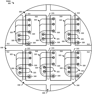
1. A method of photonics die testing, comprising:
providing a first grating coupler and a second grating coupler on a first die, a first integrated waveguide on a second die, and a first sacrificial waveguide at least partially in a scribe line between the first die and the second die of a wafer, wherein the first integrated waveguide couples directly to the first sacrificial waveguide;
providing a third grating coupler and a fourth grating coupler on the second die, a second integrated waveguide on the first die, and a second sacrificial waveguide at least partially in the scribe line, wherein the second integrated waveguide couples directly to the second sacrificial waveguide;
performing one or more first tests on the first die and the second die of the wafer via the first grating coupler, the first sacrificial waveguide, the first integrated waveguide, and the second grating coupler;
performing one or more second tests on the second die and the first die of the wafer via the third grating coupler, the second sacrificial waveguide, the second integrated waveguide, and the fourth grating coupler; and
removing the first sacrificial waveguide and the second sacrificial waveguide during separation of the first die and the second die of the wafer.
|