| CPC C09J 7/10 (2018.01) [B29C 35/0805 (2013.01); B29C 43/003 (2013.01); B29C 43/203 (2013.01); B29D 7/01 (2013.01); C09J 5/06 (2013.01); C09J 9/02 (2013.01); H01L 24/27 (2013.01); H01L 24/29 (2013.01); H01L 24/32 (2013.01); H01L 24/83 (2013.01); B29C 2035/0827 (2013.01); B29K 2063/00 (2013.01); B29K 2505/00 (2013.01); B29K 2995/0005 (2013.01); C09J 2301/208 (2020.08); C09J 2301/314 (2020.08); H01L 2224/293 (2013.01); H01L 2224/2929 (2013.01); H01L 2224/29076 (2013.01); H01L 2224/29083 (2013.01); H01L 2224/29499 (2013.01); H01R 4/04 (2013.01); H05K 3/323 (2013.01); Y10T 428/24612 (2015.01)] | 8 Claims |
|
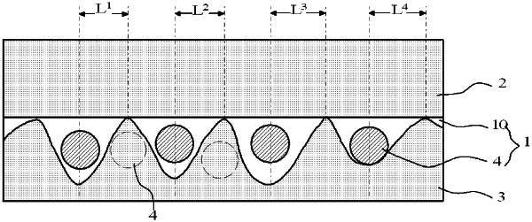
1. A method of producing an anisotropic conductive film having a three-layer structure in which a first connection layer is held between a second connection layer and a third connection layer, which are each formed mainly of an insulating resin, the method comprising the following steps (A) to (F):
Step (A)
disposing conductive particles within openings formed in a light-transmitting transfer die and placing, on the transfer die, a photopolymerizable insulating resin layer formed on a release film such that the photopolymerizable insulating resin layer faces a surface of the transfer die on which the openings are formed;
Step (B)
forming the first connection layer by applying pressure to the photopolymerizable insulating resin layer through the release film to squeeze a photopolymerizable insulating resin into the openings to thereby transfer the conductive particles onto a surface of the photopolymerizable insulating resin layer, the first connection layer having a structure in which the conductive particles are arranged in a single layer in a plane direction of the photopolymerizable insulating resin layer and in which the photopolymerizable insulating resin layer in central regions between directly adjacent conductive particles has a thickness smaller than that of the photopolymerizable insulating resin layer in regions in proximity to the conductive particles;
Step (C)
irradiating the first connection layer with ultraviolet rays through the light-transmitting transfer die;
Step (D)
removing the release film from the first connection layer;
Step (E)
forming the second connection layer on a surface of the first connection layer that is opposite to the light-transmitting transfer die; and
Step (F)
forming the third connection layer on a surface of the first connection layer that is opposite to the second connection layer.
|