| CPC B81C 1/00325 (2013.01) [B81B 7/0048 (2013.01); H04R 19/04 (2013.01); H04R 31/006 (2013.01); B81B 2201/0257 (2013.01); B81B 2207/012 (2013.01); B81C 2203/0792 (2013.01); H04R 2201/003 (2013.01)] | 20 Claims |
|
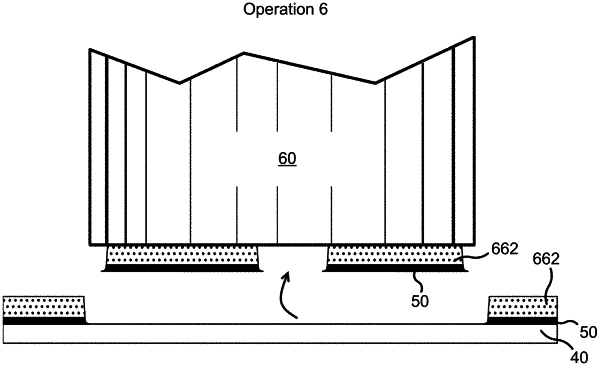
1. A method of forming a micro electro mechanical system (MEMS) assembly, the method comprising:
providing a substrate having an electrically conductive layer disposed thereon;
depositing, on the substrate over the electrically conductive layer, a bonding material having an elastic modulus of less than 500 MPa so as to form a bond layer;
completely curing the bond layer; and
attaching a MEMS die to the completely cured bond layer.
|