| CPC B81B 3/0021 (2013.01) [B81C 1/0069 (2013.01); B81C 2201/013 (2013.01); B81C 2201/0156 (2013.01)] | 14 Claims |
|
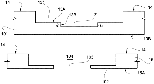
1. A process for manufacturing an optical microelectromechanical device, comprising:
forming, in a stacked arrangement, a work substrate and an insulating layer, the work substrate having a first work surface facing the insulating layer;
forming a first opening in the insulating layer;
forming a mask on top of the first work surface and the insulating layer to thereby form a second opening defined by the mask and being concentric with the first opening;
removing part of the work substrate in a region corresponding to the second opening to create a first recess, and removing the mask thereafter;
removing part of the work substrate to deepen the first recess and create a second recess surrounding the first recess and being wider than the first recess;
removing remaining portions of the insulating layer to obtain an intermediate structure, with remaining portions of the first work surface of the work substrate forming a temporary contact surface having a smaller area than the first work surface and surrounding the second recess;
thinning the work substrate while supporting the work substrate by temporarily bonding the work substrate to a supporting wafer at the temporary contact surface, the thinning serving to turn the second recess into a chamber delimited underneath by a bottom wall and serving to turn the first recess into a through recess;
blackening an outer surface of the thinned work substrate;
bonding the thinned work substrate to another temporary supporting wafer, with the bonding facing the outer surface of the thinned work substrate;
flipping the thinned work substrate and bonding the thinned work substrate on a first surface of a silicon-on-insulator wafer; and
removing the temporary supporting wafer.
|