| CPC B28D 5/0011 (2013.01) [B23K 26/0006 (2013.01); B23K 26/53 (2015.10); B28D 5/0064 (2013.01); B23K 2103/56 (2018.08)] | 21 Claims |

|
1. A production facility for separating wafers from donor substrates, the production facility comprising:
an analysis device configured to determine at least one individual property of a respective donor substrate, the at least one individual property comprising doping and/or crystal lattice dislocations of the respective donor substrate;
a data device configured to generate donor substrate process data for the respective donor substrate, the donor substrate process data comprising analysis data of the analysis device, the analysis data describing the at least one individual property of the respective donor substrate;
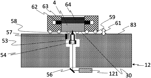
a laser device configured to generate modifications inside the respective donor substrate to form a separating region inside the respective donor substrate, the laser device being operable as a function of the donor substrate process data of the respective donor substrate; and
a separating device configured to generate mechanical stresses inside the respective donor substrate to initiate and/or guide a crack for separating at least one wafer from the respective donor substrate.
|