| CPC B23K 26/53 (2015.10) [B23K 26/0624 (2015.10); B28D 1/221 (2013.01); H01L 21/02002 (2013.01); B23K 26/40 (2013.01); B23K 2101/40 (2018.08); B23K 2103/52 (2018.08); B23K 2103/56 (2018.08)] | 25 Claims |
|
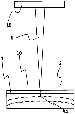
1. A method for producing a nonplanar wafer, the method comprising:
arranging a solid body in an area of a laser radiation source, the solid body delimited by a first surface portion and a second surface portion;
emitting radiation from the laser radiation source towards the solid body along a horizontal plane such that the radiation penetrates the solid body and produces a plurality of crystal lattice modifications, the crystal lattice modifications defining a first detachment region in the solid body, the first detachment region having a non-planar contour along the horizontal plane; and
separating a wafer from the solid body along the first detachment region.
|