| CPC B05B 5/007 (2013.01) [B05B 5/006 (2013.01); B05B 5/0536 (2013.01); H01T 19/04 (2013.01)] | 14 Claims |
|
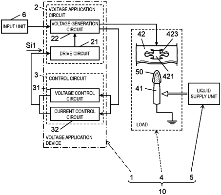
1. A voltage application device comprising a voltage application circuit that generates a discharge by applying an application voltage between a discharge electrode and a counter electrode which face each other with a clearance left from each other, wherein:
the voltage application circuit is configured to form a discharge path that is partially and dielectrically broken and located between the discharge electrode and the counter electrode when the discharge is generated,
the discharge path that is partially and dielectrically broken includes
a first dielectric breakdown region generated around the discharge electrode,
a second dielectric breakdown region generated around the counter electrode, and
a region not dielectrically broken and formed between the first dielectric breakdown region and the second dielectric breakdown region.
|