| CPC H03K 17/063 (2013.01) [H01L 27/088 (2013.01)] |

| Attention is directed to the decision of Bayerische Motoren Werke Ag et al v. Arigna Technology Limited (STAY) 1:22cv277. This reexamination may not have resolved all questions raised by this decision. See 37 CFR 1.552(c) for ex parte reexamination and 37 CFR 1.906(c) for inter partes reexamination. |
| AS A RESULT OF REEXAMINATION, IT HAS BEEN DETERMINED THAT: |
| The patentability of claims 1-2, 4, 7-8, 10, 13, 15, 17, 20, 22 and 24 is confirmed. |
| Claims 3, 5-6, 9, 11-12, 14, 16, 18-19, 21, 23 and 25-26 were not reexamined. |
|
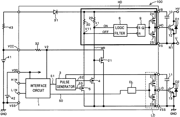
1. A semiconductor device performing drive control of first and second switching devices connected in series and interposed between a high main power potential and a low main power potential, comprising:
a high potential part including a control part configured to control conduction/non-conduction of a high side switching device which is one of said first and second switching devices;
a low side logic circuit provided in a low potential part operating on the basis of said low main power potential and configured to generate a control signal on the basis of a signal applied from outside, said control signal having a first state indicating conduction of said high side switching device and a second state indicating non-conduction of said high side switching device, and to generate first and second pulse signals on the basis of said control signal in correspondence with said first and second states, respectively;
first and second level shift parts configured to level-shift said first and second pulse signals to said high potential part to obtain first and second level-shifted pulse signals, respectively; and
a voltage detecting device provided in said low potential part and configured to detect a potential at an output line of at least one of said first and second level shift parts and to supply a logic value based on the potential for said low side logic circuit, thereby controlling an operation of said low side logic circuit.
|