| CPC H10N 10/855 (2023.02) [G01J 1/02 (2013.01); H10N 10/01 (2023.02); H10N 10/857 (2023.02)] | 15 Claims |
|
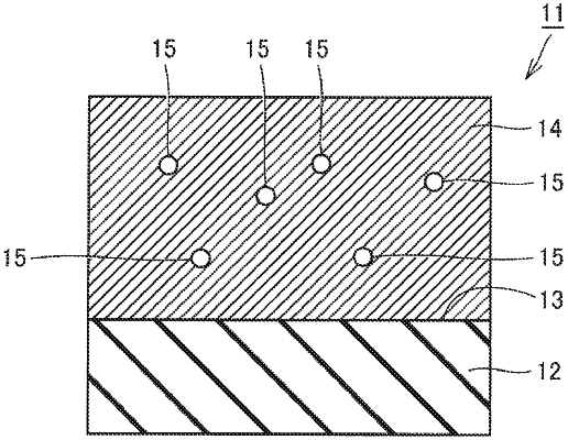
1. A thermoelectric conversion material composed of a compound semiconductor including a plurality of base material elements, the thermoelectric conversion material comprising:
an amorphous phase; and
crystal phases having an average grain size of more than or equal to 5 nm, each of the crystal phases being in a form of a grain, wherein
the amorphous phase and the crystal phases include the plurality of base material elements,
the plurality of base material elements include a specific base material element that causes an increase of a band gap of the crystal phases by increasing a concentration of the specific base material element,
an atomic concentration of the specific base material element included in the crystal phases with respect to a whole of the plurality of base material elements included in the crystal phases is higher than an atomic concentration of the specific base material element included in the compound semiconductor with respect to a whole of the plurality of base material elements included in the compound semiconductor,
a difference is more than or equal to 3 at % between the atomic concentration of the specific base material element included in the compound semiconductor with respect to the whole of the plurality of base material elements included in the compound semiconductor and the atomic concentration of the specific base material element included in the crystal phases with respect to the whole of the plurality of base material elements included in the crystal phases, and
the compound semiconductor is a SiGe-based material.
|