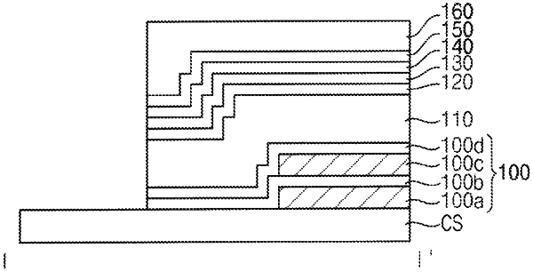
| CPC H10K 77/111 (2023.02) [H10K 59/1213 (2023.02); H10K 59/131 (2023.02); H10K 71/00 (2023.02); H10K 71/80 (2023.02); H01L 27/124 (2013.01); H01L 27/127 (2013.01); H01L 27/1218 (2013.01); H01L 27/1225 (2013.01); H01L 27/1251 (2013.01); H01L 27/1266 (2013.01); H01L 27/1288 (2013.01); H01L 29/66757 (2013.01); H01L 29/66969 (2013.01); H01L 29/7869 (2013.01); H01L 29/78675 (2013.01); H10K 59/1201 (2023.02); H10K 2102/311 (2023.02)] | 4 Claims |

|
1. A display device comprising:
a supporting substrate including a polymeric material;
a base substrate disposed on an upper surface of the supporting substrate, the base substrate including:
an organic film including a polymeric material; and
an inorganic barrier film overlapping the organic film, a width of a portion of the inorganic barrier film extending outwardly from an edge of the organic film;
a pixel array disposed in a display area of the base substrate;
a transfer wiring disposed in a bending area of the base substrate and electrically connected to the pixel array; and
an organic filling portion disposed under the transfer wiring in the bending area and contacting the organic film of the base substrate.
|