| CPC H10K 59/124 (2023.02) [H10K 50/844 (2023.02); H10K 71/00 (2023.02)] | 17 Claims |
|
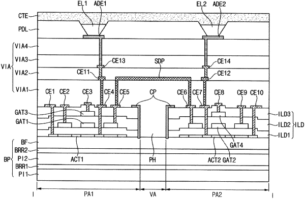
1. A display device comprising:
a substrate including a first pixel area, a second pixel area spaced apart from the first pixel area, and a valley area between the first pixel area and the second pixel area;
a first insulating layer on the substrate and in both the first pixel area and the second pixel area;
a penetration hole through the first insulating layer and corresponding to the valley area, the penetration hole exposing a side surface of the first insulating layer and an upper surface of the substrate to outside the first insulating layer;
a crack prevention pattern which is in the penetration hole and covers the side surface of the first insulating layer, the crack prevention pattern which covers the side surface of the first insulating layer being electrically floating; and
a second insulating layer facing the first insulating layer with the crack prevention pattern therebetween, the second insulating layer in contact with the upper surface of the substrate at the penetration hole.
|