| CPC H10K 50/844 (2023.02) [G09G 5/14 (2013.01); H10K 77/111 (2023.02); G09G 2354/00 (2013.01); G09G 2380/02 (2013.01); H10K 59/12 (2023.02)] | 11 Claims |
|
1. A display panel comprising:
a first region, a second region, and a display region,
wherein the first region comprises a first part of the display region,
wherein the second region comprises a second part of the display region,
wherein the second region is provided with a first component,
wherein the second region is capable of being bent with the first component facing outward,
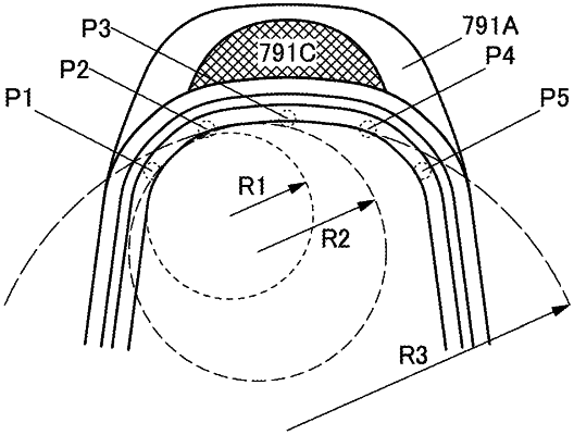
wherein the first component comprises a first elastic body and a second elastic body,
wherein an elastic modulus of the second elastic body is different from an elastic modulus of the first elastic body,
wherein the second elastic body has a top surface in contact with the second region, a bottom surface opposite the top surface, and side surfaces between the top and bottom surfaces, and
wherein the side surfaces of the second elastic body are in contact with the first elastic body both when the second region is bent and when the second region is not bent.
|