| CPC H10B 53/30 (2023.02) [G11C 11/221 (2013.01); H01L 28/56 (2013.01)] | 19 Claims |
|
1. An apparatus comprising:
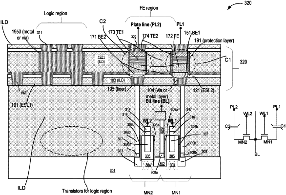
a pair of transistors, wherein a first transistor in the pair of transistors and a second transistor in the pair of transistors comprise:
a source;
a drain;
a gate electrode between the source and the drain;
a word line coupled with the gate electrode;
a drain contact coupled with the drain; and
a first via coupled with the drain contact;
a plurality of ferroelectric structures, wherein individual ones of the plurality of ferroelectric structures are electrically coupled with the first via of the individual ones of the pair of transistors, wherein the individual ones of the plurality of ferroelectric structures comprise:
a second via within a first discontinuity in an etch stop layer (ESL), and within a second discontinuity in an interlayer dielectric (ILD) over the ESL;
a capacitor on at least a portion of the second via, the capacitor comprising:
a first bottom electrode in contact with the first via;
a second bottom electrode on the first bottom electrode;
a dielectric layer comprising a ferroelectric material or a paraelectric material on the second bottom electrode;
a first top electrode on the dielectric layer; and
a second top electrode on the first top electrode; and
an encapsulation material on portions of sidewalls of a respective capacitor of the individual ones of the plurality of ferroelectric structures, and wherein the encapsulation material is not on sidewalls of the first bottom electrode of the capacitor;
a plurality of metal contacts, wherein individual ones of the plurality of metal contacts are on individual ones of the plurality of ferroelectric structures; and
a plate line coupled with the plurality of metal contacts;
a third via coupled with the source of the first transistor or the source of the second transistor, wherein the source of the first transistor is coupled with the source of the second transistor; and
a bit line coupled with the third via.
|