| CPC H10B 43/27 (2023.02) [G11C 16/0466 (2013.01); G11C 16/26 (2013.01); H01L 28/00 (2013.01); H01L 29/40117 (2019.08); H10B 43/30 (2023.02); G11C 16/0483 (2013.01); H10B 41/20 (2023.02); H10B 41/23 (2023.02)] | 20 Claims |
|
1. A semiconductor memory device, comprising:
a stacked body including:
a first stacked unit and a second stacked unit stacked above the first stacked unit, each of the first and second stacked units including a plurality of electrode layers alternately stacked with a plurality of first insulating layers therebetween, and
an intermediate insulating layer provided above the first stacked unit and below the second stacked unit; and
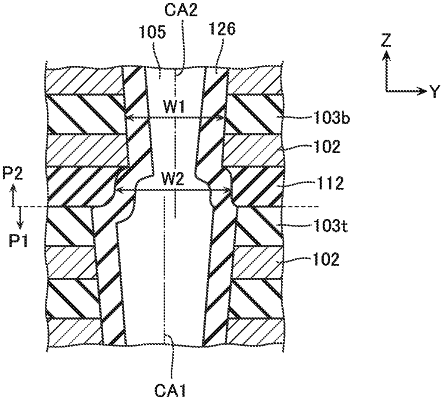
a columnar member piercing the stacked body in a stacking direction of the stacked body, the columnar member including an intermediate columnar part inside the intermediate insulating layer, wherein
a diameter of the intermediate columnar part in a first direction perpendicular to the stacking direction is broadened downwardly in an upper portion of the intermediate insulating layer as compared with a diameter of the columnar member in the first direction in a portion piercing a lowermost electrode layer of the electrode layers in the second stacked unit, a sidewall of the intermediate columnar part in the upper portion of the intermediate insulating layer having a curved shape in a cross section along the stacking direction, the diameter of the intermediate columnar part in the upper portion of the intermediate insulating layer being broadened downwardly on both sides in the first direction, and
a columnar portion included in the intermediate columnar part where the diameter of the intermediate columnar part being broadened downwardly on both sides in the first direction is formed continuously in the stacking direction.
|