| CPC H10B 41/27 (2023.02) [H01L 23/535 (2013.01); G11C 16/0483 (2013.01)] | 20 Claims |
|
1. A semiconductor device comprising:
a lower structure;
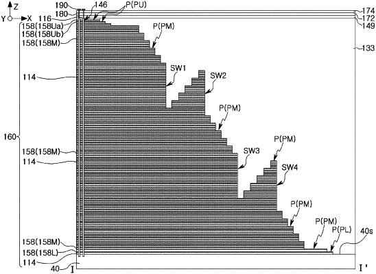
a stacked structure disposed in a first region and a second region and on the lower structure, the stacked structure including gate patterns stacked in a vertical direction, perpendicular to an upper surface of the lower structure, the stacked structure having a stepped shape in the second region; and
vertical channel structures disposed on the lower structure and penetrating through the gate patterns of the stack structure in the first region, wherein:
the stepped shape of the stacked structure includes a first downwardly stepped region, a first cliff region, a first upwardly stepped region, a second cliff region, a second downwardly stepped region that are sequentially arranged in the second region in a first direction, and
an upper end of the first upwardly stepped region is substantially at the same level as an upper region of the first cliff region.
|