| CPC H10B 10/12 (2023.02) [H10B 10/18 (2023.02)] | 20 Claims |
|
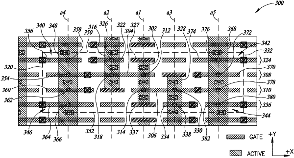
1. A memory cell, comprising:
a pair of cross-coupled inverters including:
a first transistor that includes a first active region extending along a first axis and a first gate region extending transversely to the first axis and overlaying the first active region;
a second transistor that includes a second gate region extending transversely to the first axis and overlaying the first active region, the second gate region being spaced apart from the first gate region along the first axis;
a third transistor that includes a second active region extending along a second axis and overlaying the first gate region, wherein the first active region extends across a first edge of the memory cell and a second edge of the memory cell opposite to the first edge; and
a fourth transistor that includes a third active region extending along a third axis and overlaying the second gate region;
a dummy transistor including a third gate region that overlays the first active region, the third gate region located adjacent to the first edge; and
a first read port that includes a fourth active region extending along a fourth axis, the fourth active region overlaying the first gate region.
|