| CPC H05K 1/113 (2013.01) [H05K 2201/09563 (2013.01)] | 29 Claims |
|
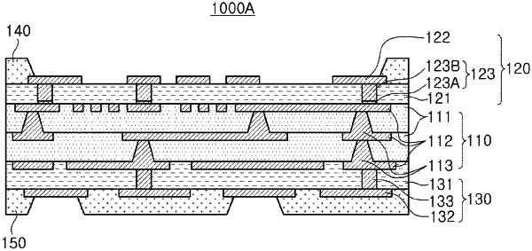
1. A printed circuit board comprising:
a first substrate portion including a first insulating layer and a first wiring layer; and
a second substrate portion disposed on the first substrate portion and including a second insulating layer, a pad disposed on an upper outer surface of the second insulating layer, and a first via penetrating through the second insulating layer and connecting the first wiring layer and the pad to each other,
wherein the first via has a boundary with each of the first wiring layer and the pad, and includes a first metal layer and a second metal layer disposed on different levels, and
the first wiring layer directly contacts a lower surface of the second insulating layer.
|