| CPC H04N 25/709 (2023.01) [H04N 23/665 (2023.01); H04N 25/745 (2023.01); H04N 25/7795 (2023.01)] | 11 Claims |
|
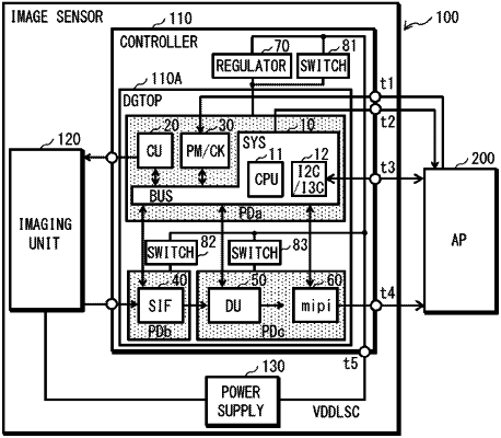
1. An imaging device comprising:
a controller configured to control an imaging unit, on a basis of a command and data that are received from a host in accordance with an I2C/I3C communication protocol;
a power supply configured to supply a voltage to a digital block of the controller, the digital block being configured to be subjected to dynamic voltage frequency scaling within one-frame operation; and
a regulator and a switch that are provided between the digital block and the power supply, and coupled in parallel with each other.
|