US 11,758,271 B2
Lens moving unit comprising a sensing magnet and a correction magnet
Tae Jin Jung, Seoul (KR); and Sang Jun Min, Seoul (KR)
Assigned to LG INNOTEK CO., LTD., Seoul (KR)
Filed by LG INNOTEK CO., LTD., Seoul (KR)
Filed on May 9, 2022, as Appl. No. 17/662,604.
Application 17/662,604 is a continuation of application No. 17/194,966, filed on Mar. 8, 2021, granted, now 11,356,609.
Application 17/194,966 is a continuation of application No. 16/541,815, filed on Aug. 15, 2019, granted, now 10,972,666, issued on Apr. 6, 2021.
Application 16/541,815 is a continuation of application No. 15/959,951, filed on Apr. 23, 2018, granted, now 10,425,585, issued on Sep. 24, 2019.
Application 15/959,951 is a continuation of application No. 15/373,032, filed on Dec. 8, 2016, granted, now 9,979,888, issued on May 22, 2018.
Application 15/373,032 is a continuation of application No. 14/643,414, filed on Mar. 10, 2015, granted, now 9,547,216, issued on Jan. 17, 2017.
Claims priority of application No. 10-2014-0030866 (KR), filed on Mar. 17, 2014.
Prior Publication US 2022/0264012 A1, Aug. 18, 2022
This patent is subject to a terminal disclaimer.
Int. Cl. H04N 23/68 (2023.01); G03B 13/36 (2021.01); G02B 7/08 (2021.01); G02B 27/64 (2006.01); H04N 23/55 (2023.01); H04N 23/67 (2023.01)
CPC H04N 23/687 (2023.01) [G02B 7/08 (2013.01); G02B 27/646 (2013.01); G03B 13/36 (2013.01); H04N 23/55 (2023.01); H04N 23/67 (2023.01); H04N 23/6812 (2023.01)] 20 Claims
OG exemplary drawing
 
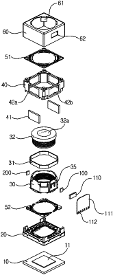
1. A lens moving unit comprising:
a cover member comprising an upper plate and a lateral wall extending from the upper plate;
a bobbin disposed in the cover member;
a coil disposed on the bobbin;
a driving magnet disposed between the lateral wall of the cover member and the coil;
a sensing magnet disposed on the bobbin;
a circuit substrate disposed on the lateral wall of the cover member; and
a sensor disposed on the circuit substrate and configured to detect the sensing magnet,
wherein the circuit substrate is disposed on an outer surface of the lateral wall of the cover member, and
wherein the sensor is disposed on an inner surface of the circuit substrate so that the sensor is not exposed outside.