| CPC H04L 27/106 (2013.01) [H04L 27/12 (2013.01); H04L 27/16 (2013.01)] | 20 Claims |
|
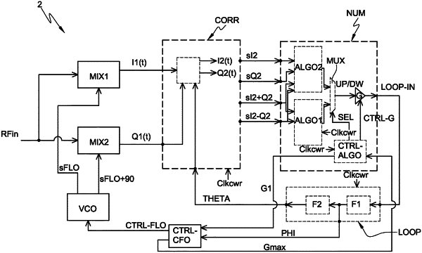
1. A device comprising:
a first circuit;
a second circuit; and
a third circuit,
wherein the first circuit is configured to:
receive a first signal,
a second signal,
a third signal, the third signal being representative of a phase shift,
generate a fourth signal and a fifth signal by applying the phase shift respectively to the first signal and to the second signal, and
deliver a sixth signal corresponding to a sampling over one bit of the fourth signal, a seventh signal corresponding to a sampling over one bit of the fifth signal, an eighth signal corresponding to a sampling over one bit of a difference between the fourth and fifth signals, and a ninth signal corresponding to a sampling over one bit of a sum between the fourth and fifth signals,
wherein the second circuit is configured to:
receive the sixth, seventh, eighth, and ninth signals,
determine, during a first phase where the first and second signals are representative of a first known symbol of a QPSK constellation, a state of a first bit from among a first state and a second state based on the eighth and ninth signals;
deliver a digital signal corresponding to a multiplication of the first bit by a gain, and
periodically decrease, during the first phase, the gain down to a unit value, and
wherein the third circuit is configured to determine the third signal based on the digital signal.
|