| CPC H04B 1/582 (2013.01) [H03H 7/463 (2013.01); H04B 1/0458 (2013.01); H04B 1/44 (2013.01); H04B 1/525 (2013.01); H04L 5/14 (2013.01)] | 20 Claims |
|
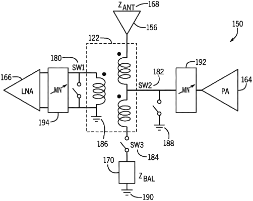
1. An electrical balance duplexer (EBD) configured to operate in either a frequency division duplex (FDD) mode or a time division duplexing (TDD) mode, the EBD comprising:
a plurality of inductors;
a transceiver comprising a receiver circuit and a transmitter circuit, the receiver circuit comprising a low noise amplifier and the transmitter circuit comprising a power amplifier;
an antenna;
a first switch on a transmission path disposed between the power amplifier and the antenna to couple the power amplifier to the antenna;
a second switch on a receiver path disposed between the low noise amplifier and the antenna; and
a third switch disposed between the antenna and a balancing impedance;
the EBD configured to:
receive communication signals at the receiver circuit, as received communication signals, and transmit communication signals at the transmitter circuit of the transceiver, as transmitted communication signals, in duplex on the antenna;
isolate the receiver circuit and the transmitter circuit via the plurality of inductors;
amplify the received communication signals from the antenna via the low noise amplifier;
amplify the transmitted communication signals to the antenna via the power amplifier;
operate in the FDD mode by opening the first switch to couple the power amplifier to the antenna, opening the second switch to couple the low noise amplifier to the antenna, and closing the third switch to couple the balancing impedance to the antenna; and
in the FDD mode, isolating the received communication signals from the transmitted communication signals.
|
|
12. A method for operating an electronic device comprising a transceiver in either a frequency division duplexing (FDD) mode or a time division duplexing (TDD) mode using a reconfigurable electrical balance duplexer, the method comprising:
receiving communication signals at a receiver circuit of the transceiver, as received communication signals, and transmitting communication signals at a transmitter circuit of the transceiver, as transmitted communication signals, in duplex on an antenna of the reconfigurable electrical balance duplexer, the reconfigurable electrical balance duplexer configured to isolate the receiver circuit and the transmitter circuit via a plurality of inductors of the reconfigurable electrical balance duplexer;
amplifying the received communication signals from the antenna by a low noise amplifier;
amplifying the transmitted communication signals to the antenna by a power amplifier;
operating the electronic device in the FDD mode by opening a first switch on a transmission path disposed between the power amplifier and the antenna to couple the power amplifier to the antenna, opening a second switch on a receiver path disposed between the low noise amplifier and the antenna to couple the low noise amplifier to the antenna, and closing a third switch disposed between a balancing impedance and the antenna to couple the balancing impedance of the reconfigurable electrical balance duplexer to the antenna; and
in the FDD mode, isolating the received communication signals from the transmitted communication signals.
|
|
15. An electrical balance duplexer (EBD) configured to:
receive reception signals at a receiver circuit and transmit transmission signals at a transmitter circuit in duplex on an antenna of the electrical balance duplexer, the electrical balance duplexer configured to isolate the receiver circuit and the transmitter circuit via a plurality of inductors of the electrical balance duplexer;
amplify the reception signals from the antenna using a low noise amplifier;
amplify the transmission signals to the antenna using a power amplifier;
communicatively decouple the low noise amplifier from the electrical balance duplexer by closing a first switch on a receiver path disposed between the low noise amplifier and the electrical balance duplexer, communicatively couple the power amplifier to the electrical balance duplexer by opening a second switch on a transmission path disposed between the power amplifier and the antenna, and communicatively decouple the antenna from a balancing impedance of the electrical balance duplexer by opening a third switch disposed between the balancing impedance and the antenna in a time division duplexing (TDD) mode when transmitting the transmission signals; and
communicatively decouple the power amplifier from the electrical balance duplexer by closing the second switch, communicatively couple the low noise amplifier to the electrical balance duplexer by opening the first switch, and communicatively decouple the antenna from the balancing impedance of the electrical balance duplexer by opening the third switch in the TDD mode when receiving the reception signals.
|