| CPC H04B 1/0078 (2013.01) [H04B 1/1615 (2013.01)] | 20 Claims |
|
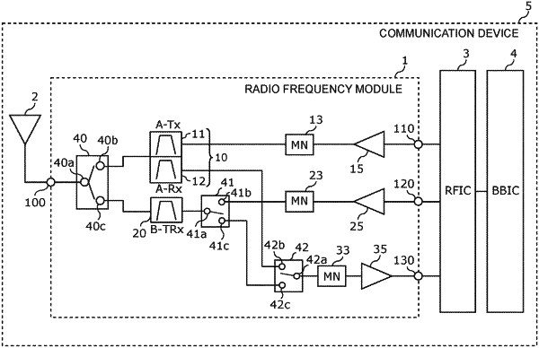
1. A radio frequency module comprising:
a first transmit filter comprising a pass band that includes an uplink operation band of a first communication band for frequency division duplex (FDD);
a first receive filter comprising a pass band that includes a downlink operation band of the first communication band;
a second filter comprising a pass band that includes a second communication band for time division duplex (TDD);
a first power amplifier configured to amplify a transmit signal of the first communication band;
a second power amplifier configured to amplify a transmit signal of the second communication band;
a low noise amplifier configured to amplify a receive signal of the first communication band and a receive signal of the second communication band;
a first switch that is configured to selectively connect the low noise amplifier to the first receive filter or the second filter;
a second switch that is configured to selectively connect the second filter to the second power amplifier or the low noise amplifier;
a first impedance matching circuit connected between the first power amplifier and the first transmit filter;
a second impedance matching circuit connected between the second power amplifier and the second switch; and
a module board comprising a principal surface, wherein
the first power amplifier, the second power amplifier, the second switch, the first impedance matching circuit, and the second impedance matching circuit are arranged on the principal surface, and
in a plan view of the module board, each of the first power amplifier, the second power amplifier, and the second switch is arranged in between the first impedance matching circuit and the second impedance matching circuit.
|