| CPC H03L 7/1806 (2013.01) [H03L 7/099 (2013.01); H04L 7/033 (2013.01)] | 20 Claims |
|
1. A circuit comprising:
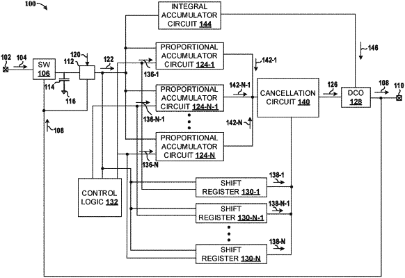
a switch configured to provide a reference input signal having a first frequency in response to an output signal having a second frequency that is greater than the first frequency;
a comparator configured to provide a series of bits based on the reference input signal and a comparator reference signal;
proportional accumulator circuits configured to provide during respective different time intervals a proportional bit based on a respective bit of the series of bits and a previously outputted proportional bit by a respective proportional accumulator circuit, the proportional bit having an instantaneous value and an average value;
shift registers configured during the respective different time intervals to shift the respective bit of the series to provide a shifted bit; and
a cancellation circuit configured to output a filtered proportional bit during the respective different time intervals based on the proportional bit and the shifted bit to remove the average value from the proportional bit.
|